Lab 1: FPGA and MCU Setup and Testing
Introduction
In Lab 1, the overall goal was to ensure our E155 Development Boards were working correctly solder all components on the board and then programming the FPGA and MCU. Both boards (FPGA and MCU) were initially programmed with example code to ensure the software flow was working. Subsequently, our task was to implement a custom design to drive a 7-segment display and several LEDs, with inputs provided through DIP switches.
FPGA Design
Steps
As shown in the Specifications, 4 DIP switch controller has to be design to control 3 LEDs and a 7-segment display. Having the following inputs and outputs:
| OUTPUT | INPUT | OPERATION |
|---|---|---|
| LED 0 | S[0:1] | XOR |
| LED 1 | S[2:3] | AND |
| LED 2 | 48 MHz clock | 2.4 Hz blink |
| 7-Segment Display | S[0:3] | binary decoder |
Aproach
I build my design using two SystemVerilog modules, one for the 7-segment display and the second one a top module that also included the led logic:
| SystemVerilog Module | Description |
|---|---|
| lab1_mb | Top FPGA specific module, includes clock module |
| sevseg | 7-segment display combinational logic |
Bellow is the design of the block diagram designed:
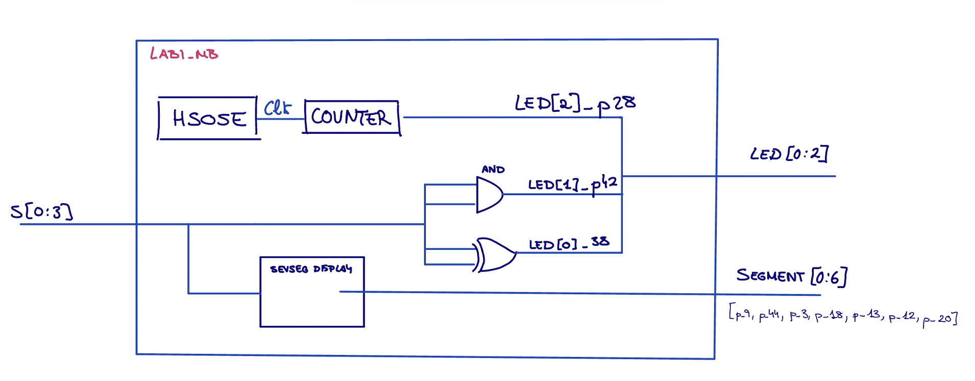
The FPGA-specific top module can be found here, and the 7-segment display module is here.
Testing
I ran into issues when running QuestaSim due to not being able to add the library iCE40 needed for the counter implementation we were using. I solved that by starting questa directly from Lattice Radiant, which did allow me to add the specific library.
Once I had Questa working, I created two testbenches to verify that my Verilog was working correctly for both modules. These testbenches load a series of testvectors that simulate all of the possible combinations of switches and checks that LEDs 0 and 1 along with the 7-segment display have the appropriate outputs.
The resulting waveforms can be found below:
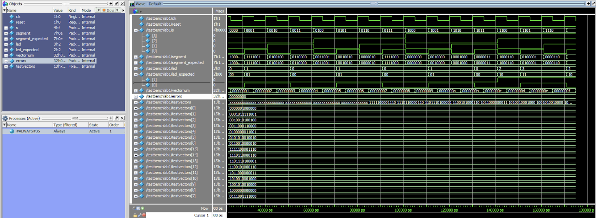
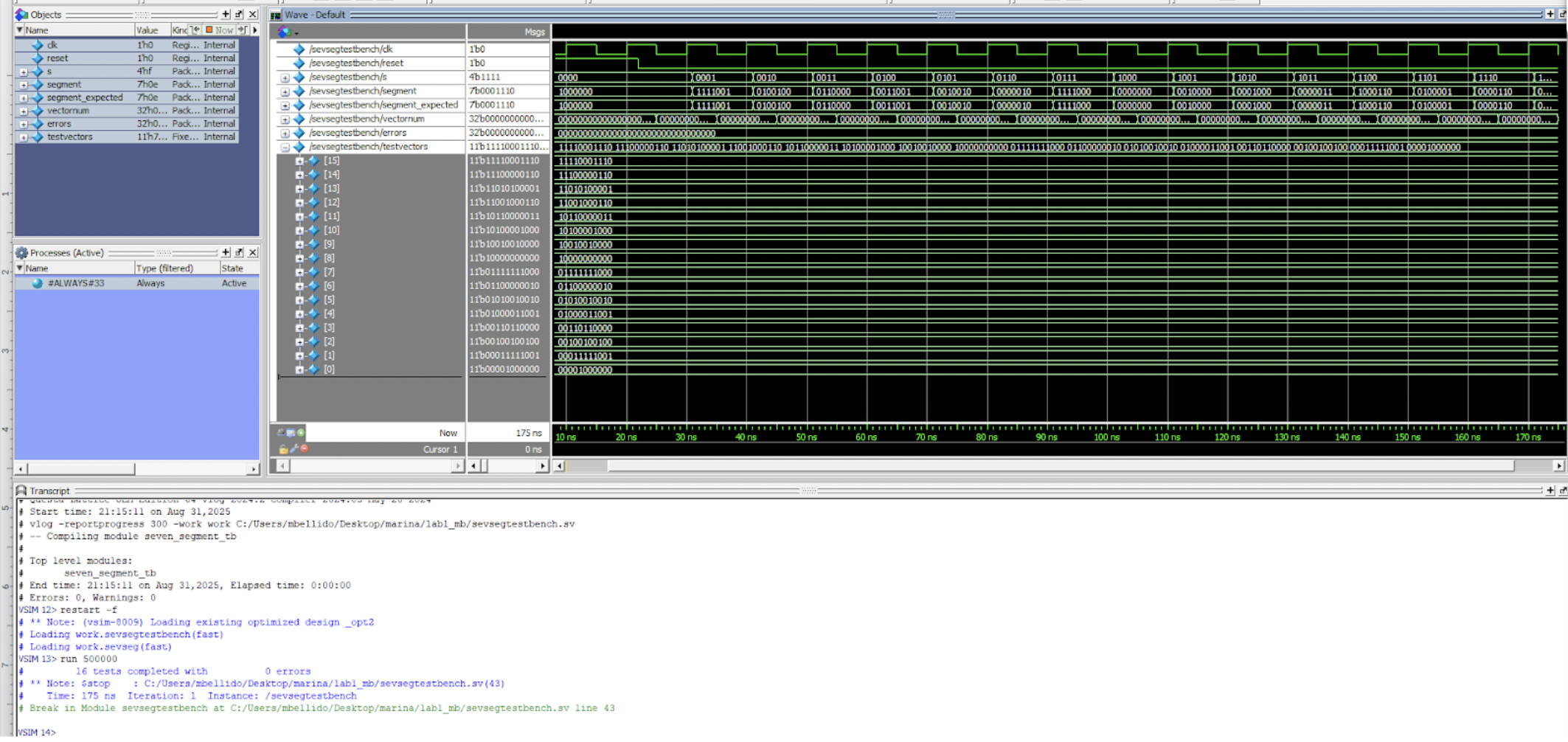
When run, the testbenches finished with the following message, indicating a successful run.
16 tests completed with 0 errors.
All testbenches and testvector files can be found here.
Hardware
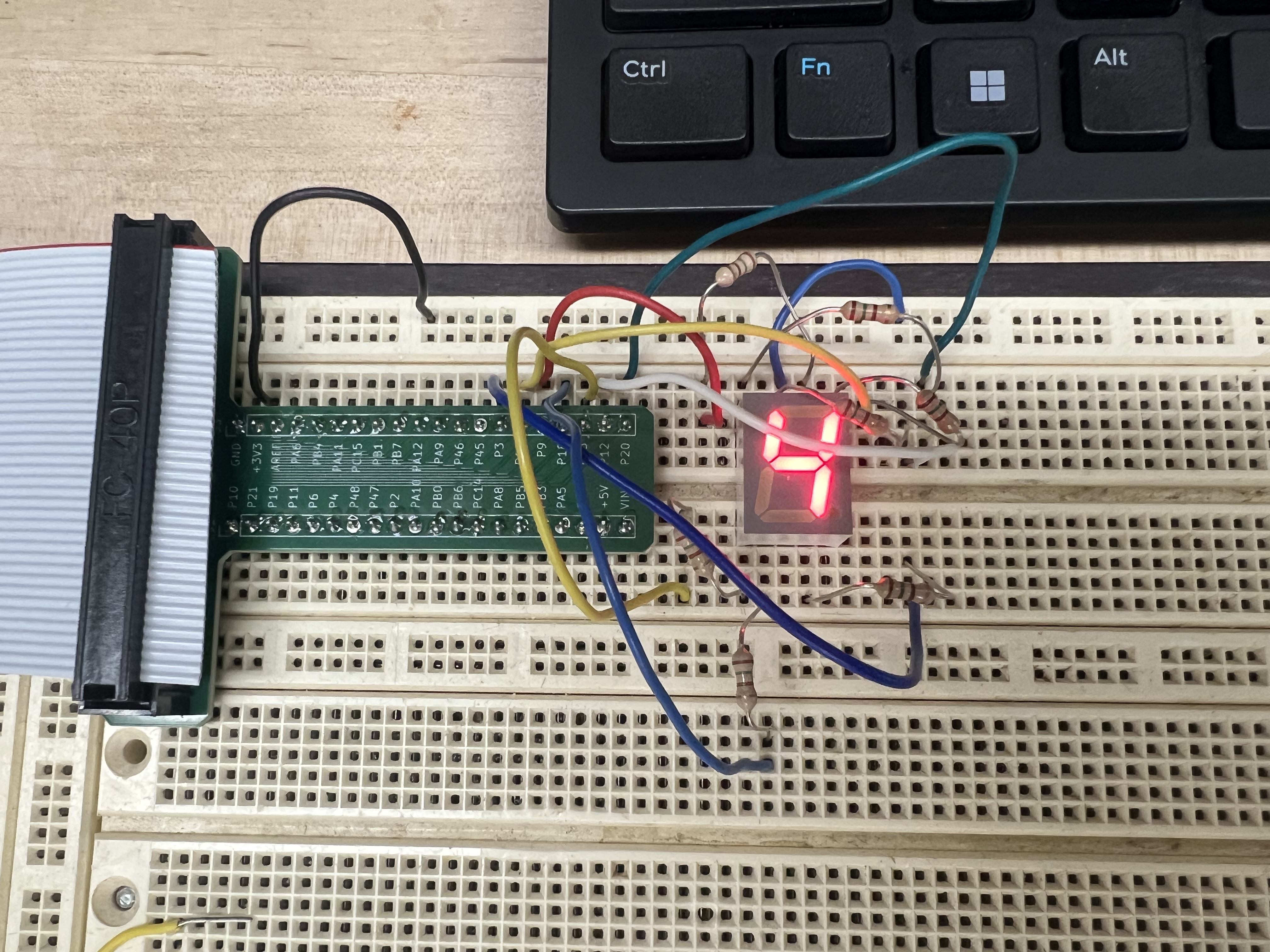
Board Assembly
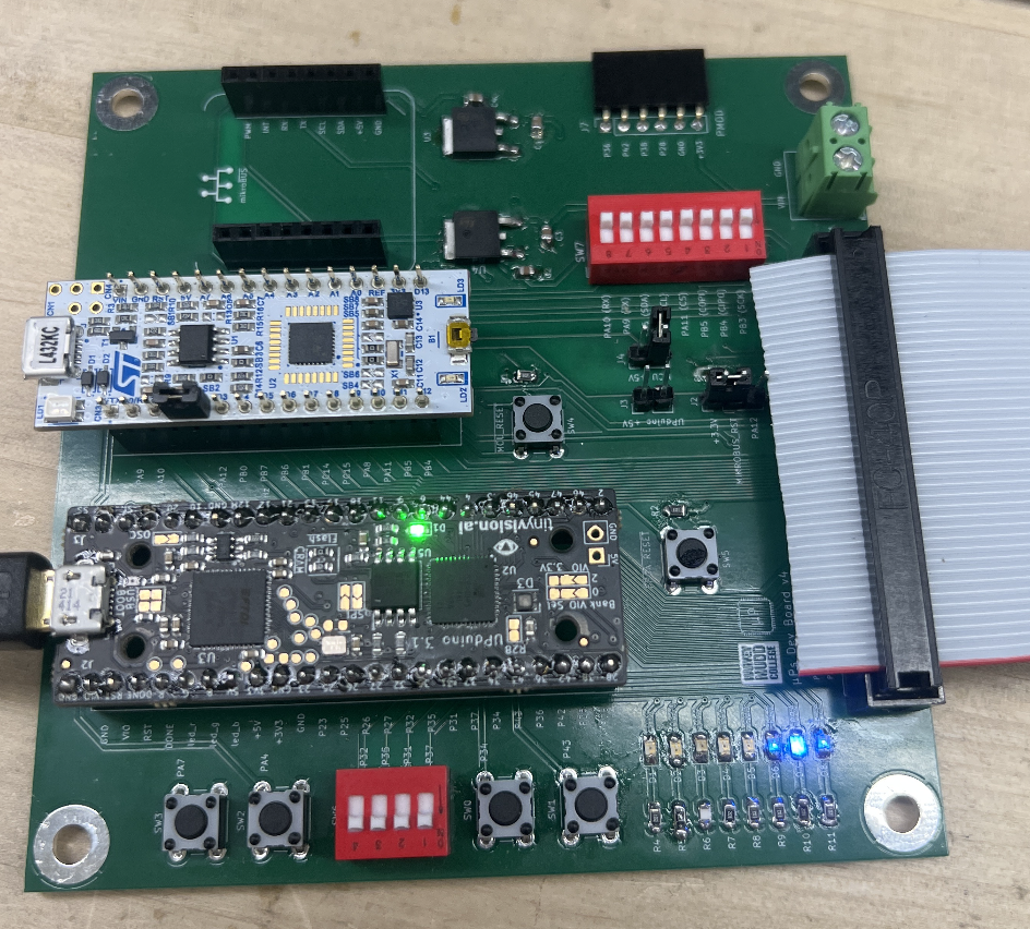
In lab1, I assembled a custom printed circuit board which hosts the MCU and FPGA boards. The board has several features that are convenient for developing embedded systems such as:
- Pins which can be directly routed from the MCU to the FPGA via the board
- Extension headers for the mikroBUS and 6-pin PMOD standard
- User configurable LEDs, pushbuttons, and slider switches.
- Header to route pins via a ribbon cable to a separate breadboard adapter PCB which can be inserted into a solderless breadboard.
After soldering all of the components to my board, I was having weird issues with the LEDS not turning on. After lots of troubleshooting, I eventually traced it down to a bad solder joint in the neighbouring resistors and after reflowing it the board was working correctly.
The assembled board can be seen here:
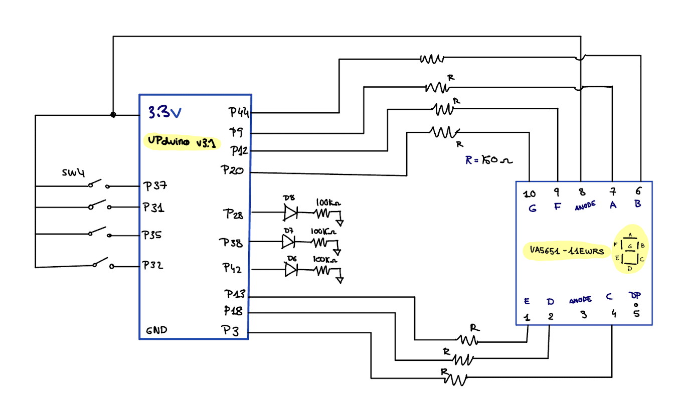
7-Segment Display circuit
The 7-segment display is a common-anode type, meaning one pin is tied to 3.3 V while the remaining pins connect through current-limiting resistors to the FPGA’s I/O. Driving an I/O pin low turns on the corresponding LED segment.
Resistor Calculation
To determine the appropriate resistor value, I used the forward voltage and current ratings from the 7-segment display datasheet. In the datasheet, the voltage drop is typically 2.1 V, so with a 3.3 V supply voltage the resistor will have 1.2 V going through it. I wanted to keep the current within the labs constraints 5-20mA to ensure low power draw so the LEDs were bright enough to see. I choose a 150ohms resistor which ended up giving me a current of 8mA (within range).
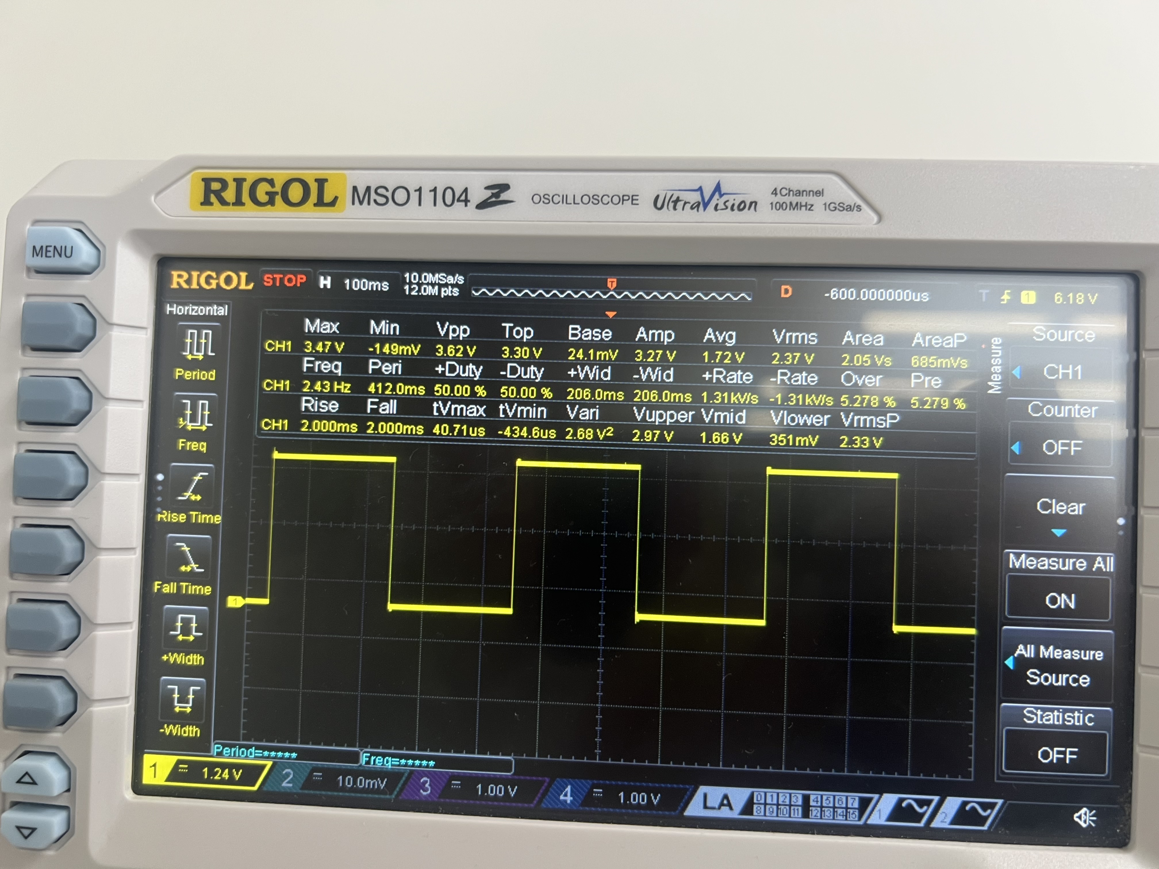
Counter Frequency Value
I used the starter code given on the website which had a clk that had a frequency of 2.4MHz and the opjective was to blink LED[2] at a frequency of 2.4Hz. To achieve that I divided the given frequency by the desired and then divided again by 2 since the clk has two edges. That resulted in 5M cycles every toggle.
Schematic
The circuit schematic consists of the FPGA, DIP switches, LEDs, and a 7-segment display.
Results
The E155 development board is fully assembled and operational. The FPGA, programmed with synthesized Verilog, drives the LEDs and 7-segment display as specified, with functionality verified in both simulation and hardware testing. The 7-segment display presents all digits clearly with uniform brightness, and overall the design meets every requirement for the lab.
AI Sections
My AI section can be found in the following link: AI SECTION